Nano-green printing technology has been extended to electronics, building materials, printing and dyeing industries. Through the innovation and application of nano-materials, the industry's environmental pollution and high energy consumption problems have been solved. At the same time, production costs have been reduced to form a "nano-material green printing industry technology cluster."
Two-section Return Printing: Nano Image Printing Technology
What exactly is nano-image printing technology? The so-called nano-image printing technology is a new type of imprinting transfer technology, which is widely used in the production of nano-embossed graphics.
Nano image printing technology is to use a mold with nano concave and convex images as a "printing plate", using silicon wafers or glass sheets coated with a polymer coating in advance as a substrate (printed object), with the cooperation of corresponding equipment and appliances, After precise imprinting and shaping, the mold is separated from the substrate. At this time, the nano-relief image present on the surface of the mold is transferred to the polymer film on the surface of the substrate without any errors. The transferred image has the same size as the concave and convex pattern on the surface of the mold, and the depth is the same. But the shape is just the opposite (yin to yang image), that is, the protrusion of the former is exactly where the latter is recessed, and vice versa. This technology that uses the principle of a printing stamp to transfer out a pattern with nano unevenness is nano-image printing technology.
Application of Nano Image Printing Technology in Packaging Printing
Two-section Return Printing: Nano Image Printing Technology
The manufacture of corrugated boxes is inseparable from packaging and printing. In the packaging and printing industry, nanoparticles play an increasingly important role. Nano ink is compatible with all aspects of performance. In product (especially food) packaging and printing, many of them have high requirements for sterilization and preservation, and traditional inks and packaging materials are blank in this regard. Nowadays, the transformation of pure natural basic materials through nanotechnology, coupled with the application of nano-ink printing, can exert amazing sterilization effects. Adding nano-silver powder to the fresh-keeping packaging materials can accelerate the oxidation of ethylene released by fruits and vegetables and reduce The ethylene content in the packaging achieves a good preservation effect. Because silicon dioxide and titanium dioxide show strong anti-ultraviolet light and catalytic performance at the nanometer scale, the nano-modified ink synthesized by special processing chemical reaction can generally improve the light resistance of 2-3 grades, and the heat resistance And the adhesion fastness has been significantly improved. By adjusting the formula, it can be made into environmentally friendly ink; adding thermal and photosensitive materials can also be made into anti-counterfeiting ink.
To summarize the application of nano image printing technology for everyone:
(1) Micro-contact printing technology (MCP)
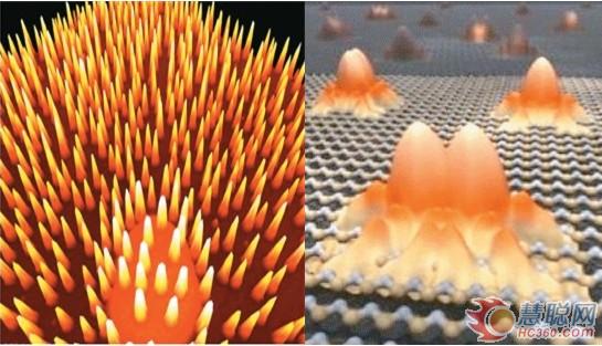
That is, the organic polymer solution is used as ink, and the image part of the silicone rubber plate is coated, and the organic polymer at the protrusion of the plate is transferred to the surface of the printed substrate by micro-contact printing (Figure 1). Due to the inventor's ingenious design, the organic polymer is firmly attracted to the surface of the substrate, forming a concave-convex image of molecular thickness. People call this technology micro-contact printing technology. It should be noted here that in the early experiments, the organic polymer ethanol solution with mercapto groups was used as the ink. The so-called substrate refers to a silicon sheet coated with a gold film on the surface. When people transfer the polymer solution containing mercapto groups on the silicone rubber plate to the gold film, a self-assembled monomolecular film image is formed. Mizutani and others from the Nanotechnology Research Department of the Japan Institute of Industrial Technology pointed out that in addition to organic polymer solutions containing sulfhydryl groups can be used as inks for microcontact printing, scientists have recently discovered aminosilanes with chemically active surfaces. It is also a very good performance ink. The image printed with this ink (the substrate is a mica sheet) was checked by atomic energy microscopy (AFM), and a large number of DNA molecules were adsorbed on the surface of the aminosilane image. It is believed that this is because the positive charge on the surface of the aminosilane and the negatively charged DNA molecules attract each other.
Micro-contact printing not only has the advantages of fast and cheap, but also does not require the harsh conditions of the clean room, or even an absolutely flat surface. Micro-contact printing is also suitable for a variety of different surfaces, with flexible and variable operating methods. The disadvantage of this method is that at the submicron scale, the diffusion of thiol molecules during printing will affect the contrast and make the printed pattern wider. By optimizing the immersion method and immersion time, especially controlling the amount and distribution of ink on the stamper, the diffusion effect can be reduced.
(2) Capillary Microstyling (MIMIC)
That is, the printing plate with the nano-concave image is placed on the surface of the substrate. At this time, the concave and convex portions of the printing plate image form a very thin gap (capillary) with the surface of the substrate, and then the liquid polymer is dropped on the silicone rubber printing plate. Due to capillary action, the liquid polymer enters these gaps by itself. If we cure the polymer in the gap and separate the two, we can obtain a fine nano-concave image. This technology can be widely used in the manufacturing field of optical components and the like. [next]
(3) Micro-transfer styling (mTM)
That is, the prepolymer is used as an ink, applied to the depression of the silicone rubber plate, and the prepolymer is transferred to the surface of the substrate by transfer, and then heated and cured to form a nano-concave image. We call this printing method micro-transfer styling.
(4) Near-field phase conversion printing (PSL)
That is, after the photoresist coating is coated on the substrate, the image is transferred on the resist coating film with a silicone rubber mold, and it is used as a mask for contact exposure, such as contact exposure with ultraviolet light. Since the uneven pattern transferred by the silicone rubber mold induces phase conversion, it is possible to form an image. However, the prerequisite is that the size of the concave and convex parts of the image is smaller than the wavelength of the ultraviolet light, and the effect of the near-field light can make the image transfer become a reality. Recently, there are reports in the literature that this technique can form nano-images on the spherical surface.
In addition to this, there is nanochemical lithography. It is one of the latest types of nanomaterial self-assembly technology. In the demonstration of the scientist, this process can effectively form a very stable periodic array of nanoparticles, without being lithography (such as atomic microscope dip printing, laser lithography, electron beam lithography, rolling) Printing, etc.) are limited by many flaws and limitations. Nano-chemical lithography involves the production of nano-sized periodic template technology, which requires absolute control over size, size, spatial distribution and function. Nanochemical lithography is a combination of multiple technologies, in which the arrangement of particles is controlled by reflecting the difference in activity, which is determined by the type of chemical treatment to which the particles and their surfaces are exposed.
Scientists use garnet red yttrium aluminum (YAG) nanoparticles polymerized on silicon chips to synthesize additive particles and crystallize them to determine their shape and composition. Before polymerizing the nanoparticles on the silicon chip, scientists used an etching technique based on the "atomic step" phenomenon to engrave the template on the silicon chip in advance. Due to the high pace of atoms that naturally exist on the surface of silicon chips, scientists can move these atoms through processing to create the required template. A thin layer of nitride formed by chemical reaction (between silicon, nitrogen, and oxygen) is correspondingly formed on the boundary of atomic steps, so that the template is pre-engraved on the chip. To align the particles along the template on the chip, the scientists placed the sample in an ultra-high vacuum chamber and annealed it for several hours. After processing at 500-850 degrees Celsius, not only the nanoparticles precisely arranged based on the template are obtained, but also another advantage is obtained. After using this technique to measure the quenching treatment, the arrangement of the nanomaterials can also show its strength. In general, many nanoparticles are exposed to photon bleaching. This damage is caused by exposure to high-intensity light; on the other hand, these particles keep theirs under the extended illumination of scientists ’fluorescence imaging measurement technology. Initial state.
Nano image printing technology is a very practical application technology. It will show its unique technical advantages in the production of nano electronic devices, nano optical components, nano bio sensors and other functional graphics with nano structures. Today, there is no doubt that nano-image printing technology will have a significant impact on the accelerated development of IT and microelectronics industry, biological and life sciences, environment and new energy technologies.
This technology has absorbed the essence of many scientific technologies such as nanotechnology, fine processing technology, contact printing technology, interface science and new materials, and was developed through in-depth research. This technology initially looks very similar to the hot stamping technology used in CD and DVD production. However, after careful comparison, it is not difficult to see that the two are obviously different. The former is only a micron-level processing technology, while the latter shows in many ways that the image is formed by the transfer (shift) at the atomic and molecular levels; the former is fine processing in the general sense, and the latter is using nanofabrication Principle, processing technology for obtaining ultra-fine graphics. If we call the former the technology of the 20th century, then the latter is undoubtedly the emerging technology of the 21st century.
The research and development of nano-image printing technology began in the mid-to-late 1990s. It was first pioneered by Professor Chou of Princeton University in the United States. After nearly 10 years of research, deepening and technical support, at present, the technology It is entering a preliminary practical stage. At the same time, Professor Chou personally organized and planned, and successively (or planned) convened a series of related international conferences (InternotionalConferenceonNanoimprintNanoprintTechnology), to promote the technology to expand and expand to the world. The first and second international conferences were held in Boston and other places in the United States in December 2002 and December 2003, respectively. Only one year later, in December 2004, the 3rd International Conference was held in Vienna, Austria. Immediately afterwards, the planned fourth conference will be held in Nara, Japan, in October 2005.
In short, nano-image printing technology has taken solid steps from theory to practice, from research and development to preliminary practical use, and its impact has spread to all parts of the world.
Spray Mop ,Spray Floor Mop,Water Spray Mop Manufacturers and Suppliers in China
China Spray mop ,Spray Floor Mop,Water Spray Mop,Microfiber Spray Mop, we offered that you can trust. Welcome to do business with us.
Hope to work with you for mutual benefits.
Spray Mop
Spray Mop,Spray Floor Mop,Water Spray Mop,Microfiber Spray Mop
Ningbo Dongsu Plastic Industry Co.,Ltd. , https://www.plasticproductmfg.com